
SEMI Standards for Wafer Handling: Key Compliance Checks
SEMI Standards for Wafer Handling: Key Compliance Checks
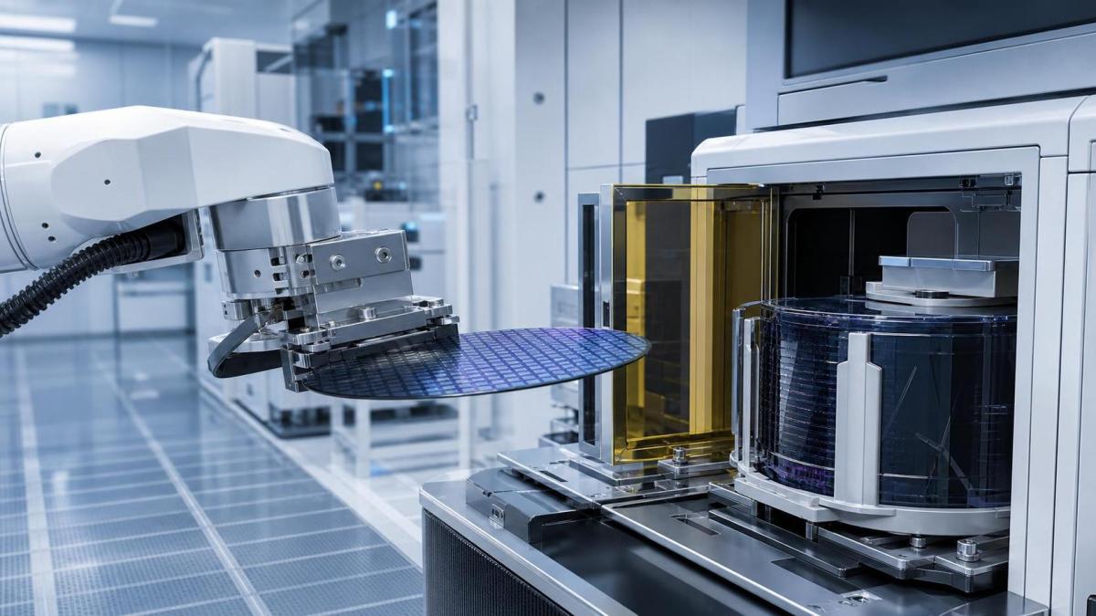
SEMI standards wafer handling requirements are where many equipment reviews stop being theoretical. On paper, most systems look clean: smooth motion, noncontact options, automation-ready interfaces, acceptable throughput. In qualification, the real questions are narrower and less forgiving. Will the end effector mark the wafer edge after repeated cycles? Does the robot maintain placement accuracy when the cassette is partially loaded? Are the materials inside the handling path actually suitable for the process environment, or just generally “cleanroom compatible”?
For technical evaluators, that is the practical value of a compliance checklist. It keeps the review tied to failure modes that matter: particle generation, electrostatic discharge, misalignment, backside contamination, wafer breakage, and undocumented changes between prototype and production configuration. The points below are written from that angle. Not as a broad primer, but as the checks people usually wish they had pushed harder during supplier assessment.
Start with the exact SEMI scope, not the sales description
Before looking at mechanics, pin down which SEMI standards are actually relevant to the tool boundary. “Compliant with SEMI” is too loose to be useful. Wafer handling reviews often touch more than one area: dimensional interfaces, communication, safety, ESD control, and equipment behavior in automated material movement. Depending on the system architecture, evaluators commonly need to check applicable documents in the SEMI E-series for equipment communication and substrate handling interfaces, and sometimes S-series requirements for safety. The exact standard set must be matched to wafer size, carrier type, automation level, and integration method. If the supplier cannot map claimed compliance to specific SEMI documents and revision levels, treat that as an early warning sign.
This sounds administrative, but it is not. A lot of downstream confusion starts here, especially when one side is reviewing FOUP-based automation and the other is quoting capability proven only on open cassette handling.
Check wafer contact strategy in detail
The first physical question is simple: where does the system touch the wafer, when, and with what repeatability?
- Edge contact should be clearly defined and limited to intended zones. Ask for the handling geometry, not just a drawing of the arm.
- If vacuum is used, verify hole pattern, suction stability, and what happens during pressure fluctuation or emergency stop.
- For Bernoulli or other noncontact concepts, ask what the actual wafer-to-tool spacing is during steady operation and during acceleration changes. “Noncontact” does not remove contamination risk if airflow disturbs particles already present in the module.
- Backside protection needs explicit review. Backside particles are often missed in early acceptance because front-side optics get more attention.
A useful habit during evaluation: request photos or microscopy images of contact surfaces after endurance cycling, if available. If they do not exist, ask for the maintenance replacement interval and the wear criteria used in the field. That answer tells you a lot about whether the supplier has lived through contamination complaints before.
Material compatibility is not the same as cleanroom suitability
This is one of the most common gaps in wafer handling assessments. Components can be low-particle in a general sense and still be the wrong choice for the chemistry, temperature envelope, purge conditions, or outgassing sensitivity of the actual process module.
Review every material inside the handling path: polymers, adhesives, cable jackets, coatings, lubricants, vacuum cups, bearing materials, and any local encapsulants. If the tool sits near ALD, CVD, etch, or high-purity gas environments, ask for documented compatibility evidence tied to that operating context. General statements like “used in semiconductor tools” are not enough. For advanced nodes or highly sensitive film stacks, even small material substitutions can change contamination behavior.
Also check whether the bill of materials is locked between tested and shipped versions. Uncontrolled substitutions in seals, tubing, or plastic parts are a recurring source of qualification surprises.
Focus on motion accuracy under real loading conditions
Published repeatability values are often measured under favorable conditions. Technical evaluators need to know what the robot or transfer stage does when the setup is slightly imperfect, because production always is.
Look for evidence covering:
- Placement repeatability across the full stroke, not only at a center point.
- Behavior with partially filled carriers, mixed wafer presence states, and expected production takt time.
- Recovery from teach-point drift, carrier offset, or slightly degraded mechanical alignment.
- Vibration sensitivity from adjacent modules or facility conditions.
If the supplier only provides a single repeatability number with no test context, the figure has limited value. What you want is the measurement method, the reference condition, and the acceptance threshold used internally. If those are unclear, mark it 【待核实】 rather than assuming the published claim maps cleanly to your line.
ESD control deserves its own review line
Electrostatic risk is often buried inside general contamination or safety discussions. That is a mistake. Wafer handling systems combine motion, surfaces, airflow, and repeated contact events, which is exactly where charge generation becomes easy to underestimate.
Ask how the supplier addresses charge dissipation at end effectors, supports, and any temporary staging positions. Verify grounding strategy and whether insulating materials exist near wafer approach zones. If ionization is part of the design, check maintenance and monitoring practices rather than accepting its presence as a complete answer. In some applications, ESD control also needs to be reviewed together with particle control because aggressive airflow mitigation can create a different contamination tradeoff.
Carrier and interface compliance has to match the factory, not just the lab setup
Whether the system handles open cassettes, SMIF pods, FOUPs, or a custom transfer arrangement, the interface review has to be grounded in the manufacturing environment where the tool will live. The practical checks are usually boring, but they are the ones that prevent line integration delays.
Cross-slot and presence detection deserve special attention. If the handling system cannot reliably distinguish those states, your downtime problem will usually show up after installation, not before.
Environmental control is part of wafer handling compliance
A handling arm does not operate in isolation. Airflow pattern, local mini-environment design, purge strategy, and module pressure behavior all affect whether an otherwise capable handling mechanism performs cleanly.
Review the contamination control concept around the transfer path. Where are particles expected to settle? Is there any recirculation zone near wafer pickup points? Does maintenance access expose surfaces that are hard to requalify afterward? For systems intended for high-purity or defect-sensitive processes, ask for the contamination verification method used during acceptance. If data is unavailable, that should trigger a site-specific validation plan rather than a paperwork waiver.
One more thing that gets missed: thermal stability. Slight thermal drift in an enclosed transfer section can show up as alignment variation long before anyone labels it a temperature issue.
Do not accept weak documentation controls
For a technical or standards-driven purchase, documentation quality is not secondary. It is part of compliance evidence. You should be able to trace the reviewed configuration through drawings, parts lists, software or firmware revision records, maintenance instructions, and validation reports.
At minimum, ask for:
- The specific standards list and revision status claimed by the supplier.
- Mechanical and material documentation covering all wafer-contact and near-wafer components.
- Test records for repeatability, detection logic, and abnormal recovery sequences.
- Change-control process for components, software, and field service modifications.
When these records are fragmented, the project usually pays for it later through longer FAT/SAT cycles and repeated clarification loops between procurement, quality, and process engineering.
A short list of red flags that should slow the decision down
Some issues do not mean automatic rejection, but they do mean the evaluator should stop treating the review as routine.
- Compliance claims without document numbers or revision references.
- Particle or accuracy data generated only on a non-production configuration.
- No clear answer on material substitutions or spare-part equivalence.
- Recovery from wafer mis-pick or interrupted transfer relies mainly on operator improvisation.
- The supplier separates communication compliance, mechanical handling, and contamination control into different teams with no integrated qualification record.
That last point matters more than it sounds. In advanced manufacturing, the failure is often not a single bad component. It is the gap between subsystems that were each “acceptable” on their own.
What experienced evaluators usually do before sign-off
They reduce the decision to a few evidence-backed questions. Is the wafer handling path physically appropriate for the substrate and process? Is the claimed SEMI compliance specific, current, and traceable? Can the system hold alignment, cleanliness, and detection performance outside ideal demo conditions? And if something goes wrong on the line, is the recovery logic controlled enough to avoid turning a minor event into scrap or downtime?
That is usually enough to separate a polished presentation from a production-ready handling solution. For teams working in the G-UPE style of evaluation, where standards review is tied to procurement risk and long-term operational integrity, SEMI standards wafer handling checks should be treated as a live technical verification exercise, not just a compliance box. The best reviews stay close to the wafer, close to the interface, and close to the records that prove what will actually be shipped.
Recent Articles
 2026.07.26SEMI Standards for Wafer Handling: Key Compliance ChecksSEMI standards wafer handling guide covering key compliance checks for contact control, ESD, materials, carriers, and motion accuracy—help evaluators reduce risk and choose production-ready systems.
 2026.07.25U.S. Adds 37 Chinese Semiconductor Equipment Firms to Export Control ListU.S. adds 37 Chinese semiconductor equipment firms to the export control list—learn how this BIS update could reshape sourcing risk, delivery planning, and compliance decisions.
 2026.07.25Industrial Innovation in Process Technology: Key Trends Shaping 2026Industrial Innovation in process technology in 2026 centers on precision, metrology, traceability, and smarter automation. Discover the trends helping manufacturers reduce risk and stay competitive.
 2026.07.24EU Draft Would Mandate Carbon Footprint Declarations for Electronic Specialty GasesEU draft would mandate carbon footprint declarations for electronic specialty gases, reshaping CBAM compliance, customs clearance, and supplier readiness. See what exporters and EU buyers must prepare now.
 2026.07.24How to Evaluate a Radiators Supplier for Quality, Lead Time, and CostRadiators supplier evaluation starts with quality, lead time, and total cost. Learn how to compare vendors with practical checks that reduce risk and improve sourcing decisions.
 2026.07.23US Tightens EAR Controls on ALD/CVD InputsUS Tightens EAR Controls on ALD/CVD Inputs: learn how new BIS export rules on precursors, SiH4, and NF3 impact semiconductor suppliers, skid exporters, and compliance planning.
 2026.07.23IEEE Nanometrology Standards: Key Compliance Points for Measurement AccuracyIEEE nanometrology standards define traceability, uncertainty, and method control for trusted measurement accuracy. Learn the key compliance points to reduce risk and compare data with confidence.
 2026.07.22EU Updates Electronic Gas Import and Transport RulesEU updates electronic gas import and transport rules with stricter UN classification, ADR labeling, and batch reporting. Learn what exporters, importers, and logistics teams must do now.
 2026.07.22How to Evaluate a Micro Injection System for Transfection AccuracyMicro injection system for transfection evaluation starts with accuracy, repeatability, and cell viability. Discover key metrics and supplier questions for smarter selection.
 2026.07.21U.S. Expands Export Controls on 37 Electronic Specialty GasesU.S. expands export controls on 37 electronic specialty gases, adding new BIS license rules and SEMI F57-0725 thresholds. See what SiH4, NF3, WF6, and BCl3 suppliers must do now.
 2026.07.21Common Process Issues in Artificial Leather Calendering and How to Address ThemArtificial leather calendering issues can cause thickness variation, streaks, wrinkles, and weak bonding. Learn the root causes and practical fixes to improve quality and reduce scrap.
 2026.07.21How to Evaluate a Nano-Indentation System Factory for Repeatability and SupportNano-indentation system factory evaluation starts with repeatability, calibration, and support. Learn how to compare suppliers, verify traceability, and choose with confidence.
 2026.07.20SEMI Tightens ALD/CVD Export RulesSEMI Tightens ALD/CVD Export Rules with stricter purity certification, clean assembly, and customs compliance requirements. See how OEMs, integrators, and buyers can avoid delays.
 2026.07.20How to Choose Temperature Controllers for Stable Process PerformanceTemperaturecontrollers selection starts with process needs. Learn how to compare control accuracy, sensor fit, outputs, and integration to improve stability, reduce drift, and protect product quality.
 2026.07.19US Adds 37 Chinese Chip Equipment Firms to Entity ListUS Adds 37 Chinese Chip Equipment Firms to Entity List: learn how the BIS move reshapes semiconductor sourcing, export compliance, and supply chain planning for global buyers.
 2026.07.19How to Evaluate Micro-Manipulation Technology for Medical DevicesMicro-Manipulation technology for medical devices: learn how to assess precision, cleanliness, integration, and compliance to reduce risk and choose a production-ready platform.
 2026.07.18EU Tightens REACH Limits for Electronic Specialty GasesEU Tightens REACH Limits for Electronic Specialty Gases: learn how the new 0.1 ppb rule impacts semiconductor imports, supplier verification, and compliance before 2027 enforcement.
 2026.07.18Intermodal Transport vs Trucking: Cost, Speed, and Risk FactorsIntermodal transport vs trucking: compare cost, speed, and risk factors to choose the right freight strategy, reduce shipping costs, and improve supply chain reliability.
 2026.07.17U.S. Adds 37 Chinese Firms to Export Control ListU.S. Adds 37 Chinese Firms to Export Control List: learn how the BIS Entity List update may affect sourcing, compliance screening, delivery timing, and precision manufacturing supply chains.
 2026.07.17How to Evaluate a Specialty Gases Supplier for Purity and Delivery ReliabilitySpecialty gases supplier evaluation starts with purity, packaging control, and delivery reliability. Learn the key checkpoints to reduce risk and choose a dependable partner.
 2026.07.16How to Evaluate Sub-Nanometer Manufacturing for Precision ComponentsSub-nanometer manufacturing for precision components explained: learn how to assess metrology, process stability, materials, and supplier risk for smarter sourcing.
 2026.07.15CBP Sets New HTS Code for Piezo ValvesCBP Sets New HTS Code for Piezo Valves: learn how the August 1 reclassification to HTS 8481.80.50 impacts imports, duty treatment, GSP eligibility, and compliance steps before July 31.
 2026.07.15Laser Interferometer Systems Alignment: Common Errors and FixesLaser interferometer systems alignment often fails due to beam offset, thermal drift, and weak mounts. Discover common errors, practical fixes, and proven steps to restore stable, accurate measurement.
 2026.07.15Ultra-Precision Manufacturing: Key Cost Drivers and Quality TradeoffsUltra-precision manufacturing cost drivers go far beyond unit price. Learn how materials, metrology, and supplier capability affect quality, risk, and total cost.
 2026.07.15When a Rapid Prototyping Company Speeds Up Product ValidationA rapid prototyping company speeds product validation by turning design concepts into testable parts fast, helping teams cut risk, avoid rework, and make smarter launch decisions.
 2026.07.15Piezo Quantum Stage Accuracy: What Really Limits Motion Performance?Piezo quantum stage accuracy depends on more than resolution. Learn how drift, feedback, control, and integration shape real motion performance before you buy.
 2026.07.15How to Choose a Hydraulic Press for Sheet Metal Without OverpayingHydraulic press for sheet metal buying guide: compare tonnage, repeatability, tooling fit, and lifecycle cost to avoid overpaying and choose a press that truly fits production.
 2026.07.14ArF Photoresist Chem Prices Jump 12% After Korean FireArF Photoresist Chem prices jump 12% after a Korean fire, with lead times stretching to 14–18 weeks. Learn what this means for semiconductor buyers, wafer fabs, and supply planning.
 2026.07.14Singapore Extends Traceability Rule to X-ray MetrologySingapore extends traceability rules to X-ray metrology from Sept 2026. Learn how IMDA import licensing, NIST/A*STAR calibration certificates, and compliance changes impact suppliers and buyers.
 2026.07.14CBP Sets New HTS Code for Nano-Positioning StagesCBP sets new HTS code 9031.90.85 for nano-positioning stages, cutting MFN duty from 4.2% to 0% while adding ISO 14224 clearance rules. See who is affected and what to do before August 1.
 2026.07.14SEMI F47-2026 Tightens ALD/CVD Skid ComplianceSEMI F47-2026 tightens ALD/CVD skid compliance with real-time MFC audit logging and remote calibration traceability. Learn what changes before Oct 1, 2026 for CE, UL, and KC readiness.
 2026.07.14Japan Tightens Etching Precursor Export ReviewsJapan Tightens Etching Precursor Export Reviews: learn how METI’s new controls on HF, ClF₃, and NF₃–N₂O may disrupt semiconductor supply chains, advanced foundries, and delivery planning.
 2026.07.14Glamping Units: Common Specification Mistakes That Raise Operating CostsGlamping units can look cost-effective upfront but drive higher long-term expenses. Discover the key specification mistakes that increase energy, maintenance, and downtime costs.
 2026.07.14PV Modules in 2026: Efficiency, Degradation, and ROI Benchmarks to WatchPV modules in 2026: compare efficiency, degradation, and ROI benchmarks to identify bankable solar assets, reduce long-term risk, and make smarter procurement decisions.






















FILTER_CORE
REF_NO: 0042
Editors' Picks
- 00
0000-00
SEMI Standards for Wafer Handling: Key Compliance Checks - 00
0000-00
U.S. Adds 37 Chinese Semiconductor Equipment Firms to Export Control List - 00
0000-00
Industrial Innovation in Process Technology: Key Trends Shaping 2026 - 00
0000-00
EU Draft Would Mandate Carbon Footprint Declarations for Electronic Specialty Gases